研究内容 Research
日本語版/Link to Japanese.
Updated on Feb. 8th, 2023.
We need to stop using fossil fuels as soon as possible and switch to renewable energy to quickly stop global warming and minimize the damage. Solar energy has the greatest potential and should be used as much as possible. Solar power has presumably surpassed 1 TW of installed capacity worldwide [1] and is contributing to the reduction of greenhouse gas emissions. However, since the output is affected by weather conditions, it is desirable to level the output by combining energy storage and other means for further large-scale deployment. Among the leveling methods, water electrolysis, which produces hydrogen, has the advantage that hydrogen can be used not only as a fuel but also as a chemical raw material. However, the challenge is that the price of such green hydrogen is extremely high. Since the price of hydrogen is dominated by the price of electricity [2], the cost of electricity must be reduced by lowering the cost of solar cells to make solar-powered green hydrogen economically viable. Another promising application of solar cells is solar-powered vehicles that decarbonize cars. According to demonstration tests, a plug-in hybrid vehicle equipped with solar cells with an efficiency of 34% can travel 29.1 km per day without external charging [3]. However, solar cells with efficiencies of 30% or higher are expensive. This would make cars very expensive. Therefore, there is a need for high-efficiency solar cells with dramatically lower costs.
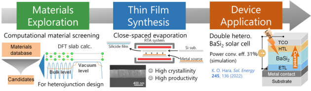
We are developing solar cells using new materials with the belief that material innovation is the key to dramatically reducing the cost and increasing the efficiency of solar cells. In particular, we are focusing on BaSi2, which has an ideal bandgap (1.3 eV) for solar cells, high light absorption ability, and is made of elements abundant in the earth. Although most solar cells currently on the market use crystalline silicon as the light absorbing material, crystalline silicon has the disadvantage of poor light absorbing ability, requiring wafers as thick as 100–200 µm to absorb enough sunlight. This limits the price reduction of solar cells. It also limits the theoretical limit of power conversion efficiency to 29–30%. On the other hand, BaSi2 can absorb enough sunlight with a 2 µm thin film, and its theoretical efficiency limit (32%) is higher than that of crystalline silicon [4]. Therefore, BaSi2 is expected to realize solar cells with higher efficiency and much lower cost than crystalline silicon. We have investigated SnS/BaSi2 heterojunction solar cells and successfully generated electricity [5]. However, the efficiency was very low due to chemical reactions at the interface. Therefore, we are currently working on the development of double heterojunction solar cells with inert interfaces, which can operate at almost theoretical limit efficiency according to device simulation [4].
However, the development of new material devices, not limited to solar cells, takes a long time. In the conventional development process, promising materials are identified through literature searches, a film deposition method is developed, the physical properties of the film are investigated, and the device application is studied. If the device properties are excellent, a productive deposition process is developed, and then the device is commercialized. Each of these steps requires optimization of the process, and if the expected properties are not achieved, the material must be reexamined. This whole process takes an enormous amount of time due to numerous trials and errors. To minimize the damage caused by global warming, we need to develop high-performance devices as quickly as possible. Therefore, we are also working to develop methods to streamline the development of new material devices.
The first method for streamlining the development of new material devices is computational material screening, which streamlines the material search. The conventional manual literature search usually limits the scope of the search. In addition, the researcher’s knowledge and experience can introduce a bias that may cause promising materials to be overlooked. On the other hand, when materials are automatically screened from a materials database using a computer program, it is possible to objectively and automatically narrow down materials that meet the requirements from a huge amount of materials data. We have used such a computational material screening approach to find suitable materials for the electron and hole transport layers of double heterojunction BaSi2 solar cells from more than 140,000 materials data [4]. A unique feature of our approach is that we incorporate not only the physical properties of the material itself, but also the interface properties of the heterojunction into the material selection criteria. We believe that this approach can be applied not only to solar cells, but also to the design of various devices to accelerate their development.
The second is the development and improvement of film deposition methods that will streamline the process of device development. For fundamental research on material properties, low-productivity epitaxial growth methods such as molecular beam epitaxy are often chosen because of the need for high-quality single crystals. On the other hand, for commercialization, methods suitable for large-area deposition, such as chemical vapor deposition and sputtering, are required, because high productivity is also important. As a result, two or more deposition methods must be developed in the process of device development, and a great deal of time is required to optimize the deposition conditions for each method. Therefore, we are working to develop a deposition method that combines epitaxial growth and high productivity, which can be used seamlessly from fundamental research to commercialization. One of our efforts is to develop a thermal evaporation method for BaSi2. We have shown that it is possible to achieve both high deposition rates of 1 µm/min and epitaxial growth [6,7]. However, thermal evaporation is not easily scalable to large area deposition. Therefore, we have developed a method that combines epitaxial growth and scalability: the close-spaced evaporation method. We have demonstrated the deposition of silicide-related materials such as BaSi2 and CaGe2 by close-spaced evaporation [8,9], and are investigating applications to other material systems.
Thus, the scope of our laboratory ranges from materials exploration to device application (see figure below). In addition to experiments, we actively use first-principles calculations and other computer simulations. Currently, we are working most intensively on the development of double heterojunction BaSi2 solar cells to demonstrate the effectiveness of computational material screening, thermal evaporation and closed space evaporation methods, and to contribute to the decarbonization of our society by developing highly efficient and inexpensive solar cells.
[1] Humans have installed 1 terawatt of solar capacity, generated over 1 petawatt of solar electricity in 2021, PV magazine, March 14, 2022.
[2] IRENA (2021), Making the breakthrough: Green hydrogen policies and technology costs,International Renewable Energy Agency, Abu Dhabi.
[3] M. Yamaguchi, et al., Prog. Photovolt. 29, 684 (2020).
[4] K. O. Hara, Sol. Energy 245, 136 (2022).
[5] K. O. Hara, et al., Thin Solid Films 706, 138064 (2020).
[6] K. O. Hara, et al., J. Appl. Phys. 120, 045103 (2016).
[7] K. O. Hara, et al., Mater. Sci. Semicond. Process. 72, 93 (2017).
[8] K. O. Hara, et al., Mater. Sci. Semicond. Process. 113, 105044 (2020).
[9] K. O. Hara, et al., Mater. Sci. Semicond. Process. 132, 105928 (2021).
日本語版
地球温暖化を早く終息させ被害を最小化するためには、できる限り早く化石エネルギーの利用を止め、再生可能エネルギーにシフトする必要があります。太陽光エネルギーは、再生可能エネルギーのうち賦存量が最大であり、これを活用しない手はありません。すでに、太陽光発電の導入量は世界で1 TWを超えたと考えられており [1]、温室効果ガス排出の削減に貢献しています。しかし、出力が天候に左右されるため、更なる大規模な導入には地域によっては蓄電などを組み合わせて出力を平準化することが望まれます。平準化方法の中でも、余剰電力で水を電気分解し水素として蓄える方法は、水素を燃料としてだけではなく化学原料としても利用できる利点があります。しかし、こうして作られるグリーン水素の価格は非常に高いことが課題です。水素価格の一番の支配要因は電力価格であるため [2]、太陽光発電によるグリーン水素を経済的に成り立たせるためには太陽電池の飛躍的な低コスト化による電力コストの低減が必要です。一方、太陽電池の自動車への搭載は、自動車の脱炭素化に貢献できる方法です。実証試験によれば、プラグインハイブリッド自動車に効率34%の太陽電池を搭載すれば、1日29.1kmを給電なしに走行できます [3]。しかし、現在実用化されている効率30%以上の太陽電池は高価で、自動車が極めて高価になってしまいます。そこで、飛躍的に低コストな高効率太陽電池が求められます。
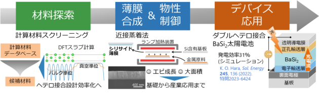
私たちは、太陽電池の飛躍的な低コスト化・高効率化をもたらせるのは材料の革新であると考え、新しい材料を用いた太陽電池の開発を進めています。特に、太陽電池に理想的なバンドギャップ(1.3 eV)と高い光吸収能を持ち、かつ、資源豊富な元素から成るBaSi2の太陽電池応用を目指した研究に最も注力しています。現在市販されている太陽電池のほとんどは結晶シリコンを光吸収層に用いていますが、結晶シリコンは光吸収能が低く、十分に光を吸収するためには100–200 µm程度の厚いウエハーが必要となる欠点があります。これが、太陽電池の価格低下を制限しています。また、発電効率の理論限界も29–30%に制限されます。一方、BaSi2は2 µmの薄膜で十分に太陽光を吸収できますし、理論限界効率(32%)も結晶シリコンより高い値です [4]。したがって、BaSi2により、結晶シリコンより高効率で圧倒的に低コストな太陽電池を実現できると期待できます。これまでに、硫化スズとのヘテロ接合太陽電池を研究し、発電に成功しました[5]。しかし、界面での化学反応のため、非常に低い効率でした。そこで、現在は、界面の安定性を考慮しつつ、ほぼ限界効率での発電をシミュレーションできるダブルヘテロ接合型太陽電池の開発に取り組んでいます[4、特開2023-6424]。
ただし、太陽電池に限らず、新材料デバイスの開発にはとても時間がかかります。従来の開発プロセスでは、文献調査で有望な材料を見つけ、成膜法を開発して膜の物性を調べ、デバイスに応用し特性を調べます。優れた特性であれば、生産性の高い成膜プロセスを開発し、社会実装に繋げます。これらの各段階においてプロセスの最適化が必要で、また、期待した特性が得られなければ、材料の見直しが必要となるため、無数のトライアルアンドエラーのために膨大な時間を要します。地球温暖化の被害を最小化するためには、できる限り速く高性能なデバイスを開発する必要があります。そこで、私たちは新材料デバイス開発を効率化する手法の開発にも取り組んでいます。
新材料デバイス開発を効率化する手法の一つ目は、材料探索を効率化する計算材料スクリーニングです。目的とするデバイスに適した材料を探す場合、従来通りの人力の文献調査では探索範囲が限られます。また、調査者の知識・経験がバイアスとなり有望な材料を見逃すことも考えられます。一方、材料データベースからプログラムを用いて機械的に材料をスクリーニングすれば、膨大な材料データの中から条件に合致した材料を客観的に機械的に絞り込むことができます。私たちは、このような計算材料スクリーニングの手法を用いて、ダブルヘテロ接合BaSi2太陽電池の電子・正孔輸送層に適した材料を14万以上の材料データの中から見つけ出しました [4]。私たちのアプローチの特徴は、材料単独の物性だけではなく、他の材料とヘテロ接合を形成した場合の特性も材料の選択基準に取り込むことです。このような手法は、太陽電池だけでなく、様々なデバイスの設計に応用し、開発の加速に貢献できると考えています。
二つ目は、デバイス開発プロセスを効率化する成膜法の開発・改良です。通常、材料物性の基礎研究では高品質な単結晶が求められるため、分子線エピタキシー法などの生産性は低いものの高品質なエピタキシャル薄膜を作製できる方法が選ばれます。一方、社会実装においては高い生産性も重要であるため、化学気相堆積法やスパッタリング法などの大面積成膜に適した手法が求められます。そのため、デバイス開発の過程で2種類以上の成膜法の開発が必要となり、それぞれの手法に対する成膜条件の最適化のため多大な時間を要しています。そこで、我々は、基礎研究から社会実装までシームレスに利用可能な、エピタキシャル成長と高い生産性を兼ね備えた成膜法の開発に取り組んでいます。その一つとして取り組んでいるのが、BaSi2の真空蒸着法の開発です。これまでに、1 µm/min程度の高速成膜とエピタキシャル成長を両立できることを示しています [6,7]。しかし、真空蒸着法は、大面積成膜への拡張性が高くありません。大面積へのスケーラビリティを兼ね備えた手法として考案したのが、近接蒸着法です。これまでに、BaSi2、CaGe2などのシリサイド系材料の成膜を実証していますが [8,9]、それ以外の材料系への応用も検討しています。
このように、材料探索からデバイス応用まで一貫して取り組んでいることが、研究室の特徴の一つです(下図)。また、実験だけでなく、第一原理計算などの計算機シミュレーションも積極的に活用しながら研究を進めています。現在、計算材料スクリーニングと真空蒸着法・近接蒸着法の有効性を実証することと、高効率で安価な太陽電池の開発による脱炭素社会形成への貢献を目指して、ダブルヘテロ接合BaSi2太陽電池の開発に最も力を入れて取り組んでいます。
[1] Humans have installed 1 terawatt of solar capacity, generated over 1 petawatt of solar electricity in 2021, PV magazine, March 14, 2022.
[2] IRENA (2021), Making the breakthrough: Green hydrogen policies and technology costs,International Renewable Energy Agency, Abu Dhabi.
[3] M. Yamaguchi, et al., Prog. Photovolt. 29, 684 (2020).
[4] K. O. Hara, Sol. Energy 245, 136 (2022).
[5] K. O. Hara, et al., Thin Solid Films 706, 138064 (2020).
[6] K. O. Hara, et al., J. Appl. Phys. 120, 045103 (2016).
[7] K. O. Hara, et al., Mater. Sci. Semicond. Process. 72, 93 (2017).
[8] K. O. Hara, et al., Mater. Sci. Semicond. Process. 113, 105044 (2020).
[9] K. O. Hara, et al., Mater. Sci. Semicond. Process. 132, 105928 (2021).